As I discussed in my 2024 year-end article, the semiconducto...
Read More Revolutionizing the way TEM metrology data is collected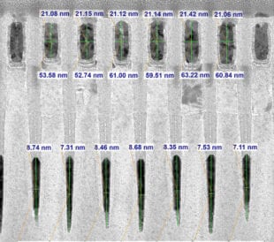
Semiconductor manufacturing stories and solutions about a more connected, more autonomous, and smarter world
As I discussed in my 2024 year-end article, the semiconducto...
Read More Revolutionizing the way TEM metrology data is collectedGrowing need for semiconductor nanoprobing As the semiconduc...
Read More Semiconductor Nanoprobing Boosts TEM Analysis Success Rates on Advanced Logic Devices
Semiconductor fabrication challenges Semiconductor fabricati...
Read More Accelerating Semiconductor Device Analysis with the Power of the Helios 5 EXL Wafer DualBeamCompound semiconductors create analytical challenges Our eve...
Read More Failure analysis of wide bandgap semiconductor devices
Dynamic random access memory (DRAM) plays a crucial role in ...
Read More Enhancing High-Volume DRAM Device Manufacturing with TEM Metrology and Characterization
Automated metrology for high-volume semiconductor manufactur...
Read More Automated Metrology Becomes a Reality with New Scanning Transmission Electron MicroscopeIt’s not an understatement to say the quality of the TEM l...
Read More Why TEM Lamella Preparation Dictates Data Quality
3D semiconductor packaging industry insights from Semicon Ko...
Read More Unraveling 3D Semiconductor Packaging ChallengesFocused ion beam scanning electron microscopes for precision...
Read More Nanoscale Microscopy with Gallium FIB SEM
Transmission electron microscopy and its increasing use in s...
Read More Transmission Electron Microscopy in Semiconductors: Generating Ground Truth Insights