Advanced metrology for 3D NAND structure manufacturing
In this blog post, learn how the design of a modern 3D NAND structure creates unique semiconductor manufacturing challenges, and the advanced 3D metrology solutions available to overcome them.
Additional resources:
Next-generation 3D NAND devices are getting taller with more layers of stacked memory cells in the vertical direction. Meanwhile, the pitch size between the memory cells continues to shrink in the horizontal direction. This three-dimensional scaling generates tall and high-aspect-ratio (HAR) 3D NAND structures that create unique manufacturing and metrology challenges.

Figure 1. 3D NAND structure manufacturing challenges at each step
Identifying 3D NAND structure manufacturing concerns
On the manufacturing side, 3D NAND devices go through several critical steps, including channel hole etch, cell deposition, die stacking, slit and staircase formation, etc. At each step, manufacturing requires a high degree of precision and process control. For instance, channel hole etch is a very exacting process that can be plagued by well-known issues such as bowing, tilt, twist, and incomplete etch as illustrated in figure 1. When these issues occur, they can result in columns touching and a corresponding bit failure.
Addressing 3D metrology data concerns
On the metrology side, fabs struggle with understanding the behavior and performance of these HAR structures due to difficulties with accessing 3D metrology data. Current solutions, such as Optical CD (OCD) and CD-SAXS, cannot provide direct measurements of small critical dimensions (CDs) hidden within the 3D structure. The main limitation is that they don’t have the ability to provide direct metrology data to accurately analyze local CD, such as channel-hole-to-channel-hole variations. This information is especially important for process development and fast yield ramp.
SEM and TEM metrology workflows for solving 3D NAND structure challenges
Fortunately, data of 3D NAND structures can be obtained by utilizing scanning electron microscopy (SEM) and transmission electron microscopy (TEM). At each process step, SEM-and-TEM-based workflows can provide direct measurements of the hidden CDs from the top to the bottom of the memory stack with sub-nanometer or sub-angstrom resolution. The data can then be used to create high-accuracy reference data, which is critical for process optimization and control. By sampling from multiple areas across the wafer, thousands of CDs per location are captured, allowing for the complete statistical analysis of critical process performance metrics like ONO layer thickness, bow CD, twist, tilt, and taper for a specific site.

Figure 2. SEM and TEM based metrology for each process step listed in Figure 1
Depending upon the process step and the required accuracy, fabs can choose either SEM-or-TEM-based metrology workflows, but often choose a combination of both to provide the most comprehensive results and solve critical challenges for all process steps as shown in Figure 2.
Although TEM-based metrology has the highest accuracy, for a few key process steps, SEM-based metrology with assistance of in-line focused ion beam (FIB) capabilities may provide a faster turnaround for obtaining high volume 3D metrology data.
Channel hole etch challenges: a SEM metrology case study
Understanding and controlling the HAR etch process relies on through-stack metrology data from the 3D NAND structures top to the bottom. A SEM metrology workflow based upon Xenon plasma FIB delayering technique solves this metrology challenge by removing material layer-by-layer while acquiring SEM images for metrology measurements. In this example, a 30 um by 30 um region of the memory array was targeted on a commercial double-deck 3D NAND device (Figure 3), and the HAR structure was delayered.
A proprietary gas chemistry was injected at the region of interest to ensure planarity and smoothness at each layer until the targeted region was delayered to the bottom of the memory stack. At each layer, a high-resolution SEM image was automatically acquired to provide metrology source images for the entire volume.
The SEM images were then analyzed with Thermo Fisher Metrology and Avizo Software to extract key parameters for 3D profiling and reconstruction.

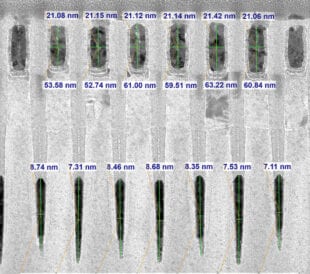
Figure 3. Targeted memory array on a commercial 3D NAND Device
The data is shown in Figure 3 and was obtained by analyzing the nearest neighbors and centers of approximately 170 memory holes in global coordinates on the SEM images through 144 layers in the targeted region.
The data tells us the average tilt increases through the stack and the local tilt varies between the left and right containers in Figure 3. In addition, the etch process is more consistent among all the memory holes at the top of the stack by showing less standard deviation compared to the bottom of each deck, and a mismatch of junction overlay (about 17 nm) at the deck interface was also captured by this technique.

Figure 4. Highly localized CD variations on commercial 3D NAND device
With this approach, fabs can make direct measurements on the memory cells through each layer to provide high-accuracy reference data for other metrology solutions, while also obtaining highly localized CD variation measurements other metrology solutions fail to provide.
This methodology provides a clear and complete understanding of in-stack parameters to inform process trend and distribution analyses. The fully automated tilting stage enables a seamless workflow of FIB delayering and SEM imaging to obtain the 3D volume data with the highest throughput. The SEM also allows the users to stop on any layers through the stack for targeted sampling and comparison, which provides more sampling as needed.
Learn more about this SEM delayering and metrology workflow conducted on the Thermo Scientific Helios 5 PXL in our 2022 FCMN Conference presentation* and our semiconductor 3D NAND whitepaper.
Thermo Fisher Scientific is the world-leading metrology solution provider for 3D NAND development and manufacturing including SEM and TEM based workflow solutions.

Infographic: Thermo Fisher Metrology Solutions for 3D NAND
*Paper presented at FCMN 2022: 3D Profiling Memory Holes with Delayering by co-authors: Zhenxin Zhong, Minkook Kim, Umesh Adiga, Arun Sundar, Melissa Mullen, Binxing Wu, Ruixin Zhang, Sean Zumwalt, David Tien

//
Xiaoting is a Sr. Market Development Manager at Thermo Fisher Scientific
Revolutionizing the way TEM metrology data is collected
As I discussed in my 2024 year-end article, the semiconducto...
Read More
Accelerating Semiconductor Device Analysis with the Power of the Helios 5 EXL Wafer DualBeam
Semiconductor fabrication challenges Semiconductor fabricati...
Read MoreFailure analysis of wide bandgap semiconductor devices
Compound semiconductors create analytical challenges Our eve...
Read More
Enhancing High-Volume DRAM Device Manufacturing with TEM Metrology and Characterization
Dynamic random access memory (DRAM) plays a crucial role in ...
Read More
Leave a Reply