It’s not an understatement to say the quality of the TEM lamella sample, or TEM lamella preparation, dictates the quality of the data that can be extracted for characterization, metrology, or failure analysis purposes.
TEM data serves as critical ground-truth information for defect analysis and yield improvements to inform technology development and semiconductor device manufacturing processes. As such, extracting accurate, high-confidence information is dependent on producing first-rate, increasingly thinner lamella.
In this blog—the third in our series on focused ion beam scanning electron microscopes (FIB-SEM)—we’ll focus on semiconductor inflection points driving the need for high-quality TEM samples and enhanced TEM data analysis, TEM lamella preparation challenges, and key features to look for in a FIB-SEM. While the examples used in this blog primarily relate to advanced semiconductors and the need for thinner samples, the recommendations are applicable to mainstream technology nodes as well.
- Blog one: Removing Large Volumes of Material Fast with FIB-SEMs
- Blog two: Nanoscale Microscopy with Gallium FIB-SEM
Semiconductor inflection points drive a need for high-quality TEM samples
Within each segment of the semiconductor industry, inflection points are occurring that are driving increased demand for high-quality TEM samples to accelerate pathfinding, failure analysis and process improvements. Some of these inflection points and associated challenges include:
- Logic: Gate-all-around (GAA) structures, such as nanosheets and forksheets, with complex three-dimension (3D) structures and line widths approaching 2nm. These advancements result in buried features that are harder to measure and difficult to find defects.
- Memory: Complex, high density, high-aspect ratio memory channels and feature shrink. Similar to logic, critical dimensions are harder to measure with smaller defects having more hiding places.
- Power: Development and integration of complex, compound semiconductor substrates such as silicon carbide (SiC) and gallium nitride (GaN). Producing compound semiconductors at a high yield rate is a complex process that may be negatively impacted by atomic-scale substrate defects.
- Mainstream technology nodes: As demand for semiconductors continues to grow, increasing fab yields for 14 nm and above is needed to meet demand and increase profitability.
Three TEM lamella preparation challenges: FIB damage, cut placement, lamella thickness
A number of factors may impact the ability to deliver high-quality, very thin lamella of 30 nm or less for TEM metrology, characterization, and failure analysis. For instance, to target one structure in a 3D device with features that wrap around, you must be within that nanometer range of the technology. A second factor may be materials that mill at different rates. A third may be the complexity of the structure itself.
To navigate these situations, it is important to be aware of three challenges that can impact the quality of the lamella: FIB damage, cut placement and lamella thickness. In the next sections, we will discuss each of these in more detail.
Focused ion beam damage
While the goal of TEM lamella preparation is to create a sample with as little damage as possible, the reality is some amount of amorphous damage will occur. The worst case, depending on the accelerating voltage used for the final polish, is that excessive damage can obscure features and defects, or render the sample unusable.
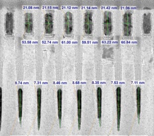
For instance, the amorphous damage to silicon is proportional at a rate of approximately one nanometer per kV. So, if you need to make a 60 nm sample and are milling at 20kV on both sides of the sample, the total damage is 40 nm. This effectively limits the value of your sample as illustrated in the figure below.

Figure 1: This image shows a comparison of the damage to one side of a sample at different voltages from 5kV to 500V. Low kV ion polishing is extremely important for lamella preparation.
As a result, and especially when trying to isolate a defect in advanced logic and memory, the ability to polish at 500V is quickly becoming a requirement.
Along with the ability to polish at a low kV, it is critical that you can see the sample even at low voltages during the FIB process. By having both, this increases the success rate when preparing the lamella. To address this need, the Phoenix FIB column available in the industry leading was designed to provide a broad range of accelerating voltages from 30 kV to a few hundred volts, and 500 nm resolution at 500 eV for high image quality at low voltages.
FIB cut placement
Accurate and controlled cut placement is a second critical capability for hitting the region of interest (ROI) and delivering the data you need. For example, if you are targeting point X, but end up at point Y, you are not going to get any of the features you care about. And if you don’t stop on the target, a defect you are searching for may be removed.
The importance of cut placement is illustrated in the figure below. In this comparison, we can see the difference of a few nanometers. In the off-center image on the left, residual SiGe stressor material obscures the feature of interest, and in the centered image on the right, the fin in a gate is perfectly centered and does not display unwanted projection artifacts.

Figure 2. Comparing an off-centered with a centered fin in a gate.
To put the cut placement in the right position, two capabilities are essential, SEM image quality and the ability to switch quickly from electron beam to ion beam.
Good SEM image quality provides the ability to take an orthogonal view of the structure as features come and go. This lets you know when a feature is approaching, when to stop and when to shift from high kV to low kV. The ability to quickly shift from electron beam to ion beam lets you make a few cuts, image to orient yourself, and then repeat until you reach the target.
Together, these capabilities, found in the industry leading Thermo Scientific Helios 5 DualBeam solutions, support accurate automated and manual end-pointing to ensure accurate cut placements.
TEM lamella thickness
A final consideration when preparing lamella is thickness. With thickness there are two elements to consider. The first is the feature size and the second is an inflection point related to the need to go super thin.
Feature size – When preparing the lamella, it is important that the thickness of the lamella is such that it does not include other features that may obscure the area you are trying to analyze.
For instance, in the figure below, you see two very thin lamella for a 14nm logic sample. The image on the left is 16nm thick and shows artifacts from the gate wrapping around the fin at the bottom. The presence of the artifact can obscure metrology like the gate oxide thickness between the gate and fin. In the image on the right, the sample thickness was reduced to 7nm enabling isolation of the feature and removal of the artifacts.

Figure 3. The 16 nm thick image of 14 nm logic device shows the artifact from the gate wrapping around the fin, while the 7 nm thick image does not.
Super thin – Up until this point, we’ve been discussing top-down lamella prep. This method is the oldest and most used method for TEM lamella preparation. However, as the need to produce super thin lamella (sub 10nm) increases, top down has its limitations and an alternative approach, inverted sample preparation is needed. The following figure is a comparison of the two methods with images to illustrate the benefits of inverted semiconductor sample preparation.

Figure 4. Curtaining from top-down lamella preparation is shown. This limits the ability to produce sub 30 nm samples for today’s advanced semiconductor devices.
With the incident ion beam coming from the top down as indicated by the yellow arrows in the image above, curtaining may occur. This is often a result of materials with dissimilar mill rates above the ROI. The smaller image on the right shows curtaining or streaks in the transistor region from the upper metallization. The occurrence of this may affect the accuracy of metrology analysis and measurements.
In this instance, even if you have something like a thin ALD layer at the surface, it is hard to achieve consistent lamella thickness with top-down preparation below approximately 30nm. This is due to low kV beam spread and the protective cap not being able to hold up during final polishing.

Figure 5. Inverted lamella preparation flips the sample to ability to produce sub 30 nm samples on today’s advanced semiconductor devices is limited due to curtaining.
In comparison, inverted sample preparation flips the sample upside down, so that the cap created on the bulk sample surface is at the bottom when attaching it to the grid. This places the ROI on top of the metal lines to prevent curtaining during milling. With this method, we also recommend implementing a wedge milling approach as seen in the orthogonal end view of the lamella to the right. This allows the user to achieve a super thin lamella at the ROI, while the upper portion of the lamella is left thick. An additional benefit is this also helps with structural stability and increases the success rate of making sub 10nm samples.
Lastly, while the inverted method may seem more complex, the thinning process is effectively the same as top down. It’s just the inversion process during liftout that’s different. Unique to the Helios 5 HX DualBeam, the sample inversion process is fully automated via AutoTEM 5 software, which reduces barriers to utilizing this technique and does not require highly skilled operators.
The Helios 5 DualBeam family: superior lamella preparation
As semiconductor technology advances, the ability to create high-quality lamella with a high success rate is critical to providing actionable TEM metrology, characterization and failure analysis data. To address the challenges associated with producing TEM samples, it is important to have tools that minimize damage to the lamella, offer high confidence cut placement capabilities, and enable you to create samples with the thickness you require for today and tomorrow’s semiconductors.
Thermo Fisher offers a broad range of gallium FIB-SEMs to meet the evolving TEM lamella preparation needs of the semiconductor industry. These include the Thermo Scientific Helios 5 FX DualBeam, the Thermo Scientific Helios 5 HX DualBeam, and Thermo Scientific Helios 5 UX DualBeam. These systems provide industry leading, precise, repeatable milling and high-resolution imaging capabilities for semiconductor sample preparation.
-

- Helios 5 FX DualBeam
-

- Helios 5 HX DualBeam
-

- Helios 5 UX DualBeam

Revolutionizing the way TEM metrology data is collected
As I discussed in my 2024 year-end article, the semiconducto...
Read More
Accelerating Semiconductor Device Analysis with the Power of the Helios 5 EXL Wafer DualBeam
Semiconductor fabrication challenges Semiconductor fabricati...
Read MoreFailure analysis of wide bandgap semiconductor devices
Compound semiconductors create analytical challenges Our eve...
Read More
Enhancing High-Volume DRAM Device Manufacturing with TEM Metrology and Characterization
Dynamic random access memory (DRAM) plays a crucial role in ...
Read More
Leave a Reply